 |
 |
 |
|---|---|---|
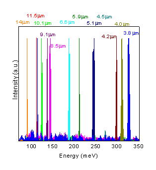
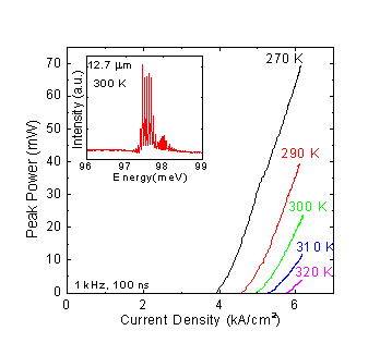
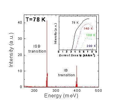
| Fig. 1 Emission spectra | Fig. 2 Current desnity-light output characteristics | Fig. 3 Simultaneous lasing of intersubband and interband transition |
| Quantum Well Intersubband Optical Devices Based on InAs, GaAs, and ZnO |
|---|
| 1. Introduction |
| Intersubband transitions in semiconductor quantum well structures (QWs) are of great interest for the optical device application such as quantum cascade lasers (QCLs), QW infrared detectors (QWIPs), and ultrafast optical switches. Our group has studied and developed QW intersubband optical devices using three kinds of materials. |
|---|
| 2. Mid-infrared InAs QCLs |
| QCLs are unipolar long-wavelength semiconductor lasers from mid-infrared to THz region utilizing carrier recycling in active region. Although fundamental properties of QCLs such as emission wavelength can be designed, the ultimate performance depends not only on the structure design but also on the material properties. Optical gain is one of the properties that depend critically on materials; small effective mass increases dipole matrix element for a given well width and reduces nonradiative relaxation rate due to the longitudinal optical (LO) phonon. We have chosen InAs/AlSb as a material for mid-infrared QCLs that provides a small effective mass (0.023m0) and high conduction band offset energy (2.1 eV) compared with other materials. Up to now, in addition to the first operation of InAs QCLs [1], we have demonstrated low threshold current density operation (Jth) at liquid nitrogen temperature [2], room temperature operation [3], and high temperature operation in the mid-infrared region [4]. Also we have showed that simultaneous lasing of intersubband and interband transition is possible in InAs/AlSb QCLs, enabling the use of two-color, two-mode emissions [5] |
|---|
|
|
|
|---|---|---|
| Fig. 1 Emission spectra | Fig. 2 Current desnity-light output characteristics | Fig. 3 Simultaneous lasing of intersubband and interband transition |
| 3. THz GaAs QCLs |
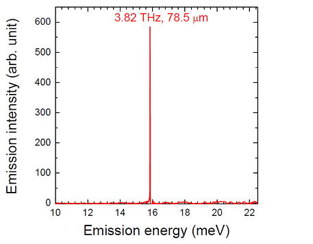
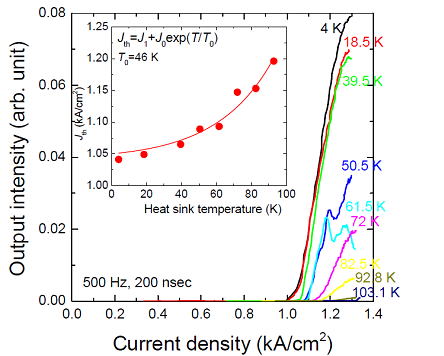
| For THz region, at present stage, GaAs/AlGaAs materials have been employed because of low residual carrier concentration and well-known band parameter. Until now we have successfully demonstrated the operation of THz QCLs (3.1-3.8 THz). The active/injection layers were designed using a LO phonon depopulation scheme. A single plasmon waveguide was used for the optical confinement. The observed lowest Jth at 5 K was 1.1 kA/cm2 and the maximum operation temperature was 103 K. In order to estimate thermally activated LO phonon scattering time which limits characteritics temperature (T0) of Jth, we analized temperature dependence of Jthexperimentally and theoretically [6]. |
|---|
 |
 |
|---|---|
| Fig. 4 THz Emisson spectra | Fig. 5 Current density-light output characteristics of fabricated sample |
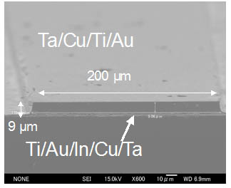
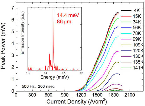
| We have also fabricated THz QCLs using Cu and Au-based metal-metal waveguide for optical confinement. The thickness of In layer used for bonding, and using dry etching method were the critical parameters for a successful metal-metal waveguide device process with high reproducibility. Result shows a decrease of threshold current density Jth at 0.8kA/cm2 and a significant increase in max imum operating temperature at 146 K. The decreased range of threshold current density is consistent with simulated result of waveguide loss. |
|---|
 |
 |
||||||||||||||||||||||||||
|---|---|---|---|---|---|---|---|---|---|---|---|---|---|---|---|---|---|---|---|---|---|---|---|---|---|---|---|
| Fig. 6 SEM image of the laser facet with Cu-Cu waveguide. | Fig. 7 Current density-light output characteristics of fabricated sample using metal-metal waveguide | ||||||||||||||||||||||||||
| 4. ZnO QWs |
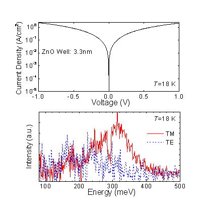
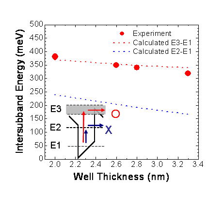
| ZnO-based QWs have the potential for intersubband QWs devices; large optical phonon energy (60 meV) can decrease the thermally activated LO phonon scattering rate which is expected to limit T0 of THz QCLs, and strong electron-phonon interaction and large conduction band offset energy make it possible to demonstrate ultrafast QWIPs at a wide spectrum range. Recently we have observed intersubband optical transitions in ZnO-based QWs for the first time [7]. All the ZnO/MgZnO QWs were grown on O-polar ZnO substrate by plasma-assisted molecular beam epitaxy [8]. The transition energies obtained from photocurrent spectra were in close agreement with the calculated transition energies. |
|---|
 |
 |
|---|---|
| Fig. 8 Low temperature current-voltage chacateristic and photocurrent spectrum of n-ZnO/MgZnO MQWs | Fig. 9 Comparison with calculation |
| References |
|---|
| [1] K. Ohtani and H. Ohno, Appl. Phys. Lett. 82, 1003 (2003). [2] K. Ohtani, K. Fujita, and H. Ohno, Appl. Phys. Lett. 87, 211113 (2005). [3] K. Ohtani, K. Fujita, and H. Ohno, Electron. Lett. 43, 520 (2007). [4] K. Ohtani, Y. Moriyasu, H. Ohnishi, and H. Ohno, Appl. Phys. Lett. 90, 261112 (2007). [5] K. Ohtani, H. Ohnishi, and H. Ohno, Appl. Phys. Lett. 92, 041102 (2008). [6] Tsung-Tse Lin, Keita Ohtani, and Hideo Ohno, Appl. Phys. Exp. 2, 022102 (2009). ]7] M. Belmoubarik, K. Ohtani, and H. Ohno, Appl. Phys. Lett. 92, 191906 (2008). [8] H. Z. Xu, K. Ohtani, M. Yamao, and H. Ohno, Appl. Phys. Lett. 89, 071918 (2006). |