Magnetic Metals and Their Applications to Nonvolatile Spin Memories

    Development of magnetic tunnel junctions (MTJs) that exhibit high tunnel magnetoresistance (TMR) ratio is needed to realize the high speed magnetoresistive-random access-memories (MRAMs), and high TMR at low resistance area (RA) product range is required for magnetic sensors in the sub Tbit/in. hard-disk-drives (HDDs) and beyond. Also Current-driven magnetization switching is preferred over conventional cross-point current-generated magnetic field writing in MRAMs, because the required absolute current scales with the area of the device. In order for this approach to be viable in the 90 nm technology node and beyond, critical current density (Jc) must be lower than 106 A/cm2 to be driven by a metal oxide semiconductor (MOS) transistor. We have developed MgO-based MTJs exhibiting large TMR ratio and low current density magnetization switching. Observed TMR ratio of our MTJ is 472% and minimum critical current density for magnetization switching is 7.8-8.8x10⁵ A/cm2 range. This work is supported by th IT-program of research revolution 2002 "Development of universal low power spin memory" from MEXT.


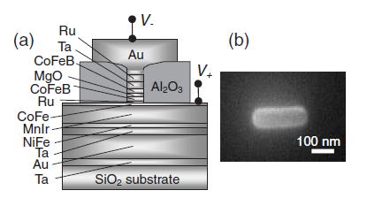
Fig. 1  Schematic drawing of cross section of fabricated MTJ. The thickness of MgO is fixed to 0.85 nm. (b) Scanning electron microscopy image of a pillar after miling showing that the area of the fabricated pillar is 80 x 240 nm2
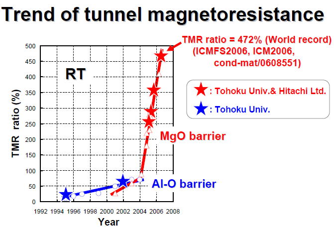
Fig. 2  Thrend of tunnel magnetoresistance of MTJ. We have realized  record tunnel magnetoresistance (TMR ratio =472 %) by using MgO-based MTJ.
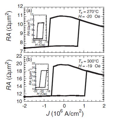
Fig. 3  Resistance area (RA) product of versus current density (J) loops at room temperature for two samples annealed (a) at 270°C (sample A) (b) at 300°C (sample B). These curves were taken under a fixed external magnetic field to compenstate the effect of the offset field.  The averaged critical current density is 7.8x10⁵ A/cm2 for sample A and 8.8x10⁵ A/cm2 for sample B.   


Publications
1. Y. M. Lee, J. Hayakawa, S. Ikeda, F. Matsukura, and H. Ohno, Appl. Phys. Lett. Vol. 89, 042506(1)-(3) (2006).
2. S. Ikeda, J. Hayakawa, Y. M. Lee, R. Sasaki, T. Meguro, F. Matsukura, and H. Ohno, Jpn. J. Appl. Phys. Vol. 44, L1442-L1445 (2005).
3. J. Hayakawa, S. Ikeda, Y. M. Lee, R. Sasaki, T. Meguro, F. Matsukura, and H. Ohno, Jpn. J. Appl. Phys. Vol. 44, L1267-L1270 (2005).
4. J. Hayakawa, S. Ikeda, F. Matsukura, H. Takahashi, and H. Ohno, Jpn. J. Appl. Phys. Vol. 44, L587-L589 (2005).