 |
| (In,Mn)As Nanostructures |
| S. P. Guo, H. Ohno, A. Shen, F. Matsukura, and Y. Ohno, "Self-organized (In,Mn)As diluted magnetic semiconductor nanostructures on GaAs substrates," Applied Surface Science, vols. 130-132, pp. 797-802, 1998. |
We have grown (In,Mn)As quantum dots QDs on GaAs (100), (211)B and (311)B substrates. The observation of reflection high energy electron diffraction pattern and atomic force microscopy measurement confirmed the formation of the (In,Mn)As QDs. The structure grown on GaAs (100) showed a broad range of dot sizes with irregular shape. For the structure grown on GaAs (311)B, (In,Mn)As QDs with bimodal size distribution were observed. The (In,Mn)As QDs grown on GaAs (211)B showed improved size uniformity compared to those grown on GaAs (100) and (311)B.
|
| Fig. 1. RHEED patterns of (a) GaAs (100) buffer layer, (b) 2 ML of (In,Mn)As on GaAs (100) right after growth, (c) 8 ML of (In,Mn)As on GaAs (100) right after growth and (d) 8 ML of (In, Mn)As on GaAs (100) after 60 s growth interruption. All taken along [011] azimuth at 350oC |
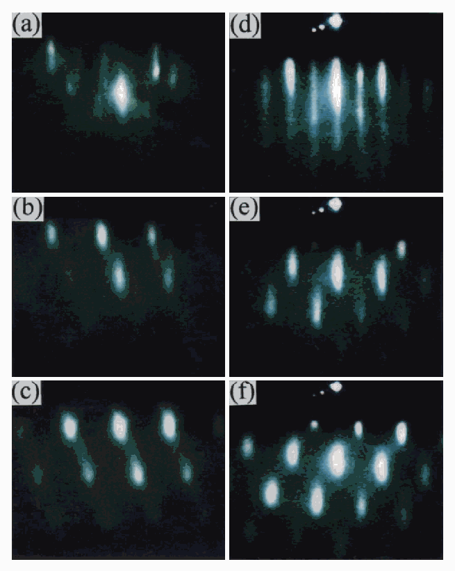 |
| Fig. 2. RHEED patterns of (a) GaAs (211)B buffer layer, (b) 6 ML211 of (In,Mn)As on GaAs (211)B right after growth and (c) 6 ML211 of (In, Mn)As on GaAs (211)B after 60 s growth interruption, (d) GaAs (311)B buffer layer, (e) 5 ML311of (In,Mn)As on GaAs (311)B right after growth and (f) 5 ML311 of (In, Mn)As on GaAs (311)B after 60 s growth interruption. All taken along [011] azmith at 350oC. |
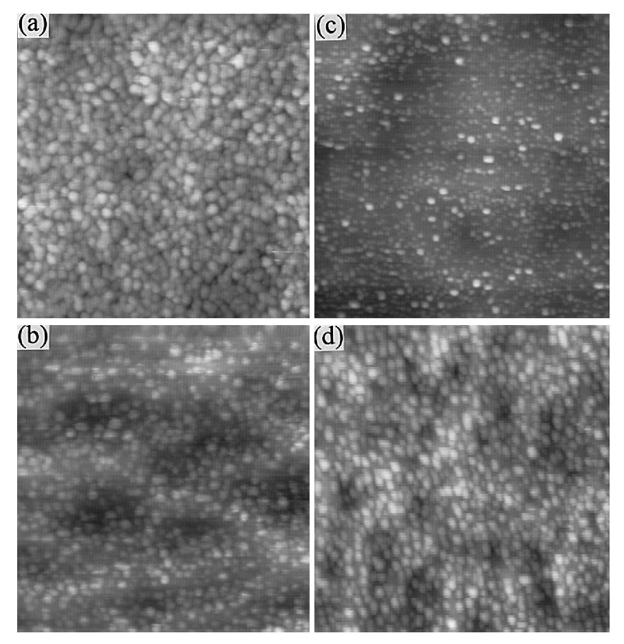 |
| Fig. 3. 1x1 µm² AFM images of (a) 8 ML of (In, Mn)As grown on GaAs (100), (b) 6 ML211 of (In,Mn)As grown on GaAs (211)B, (c) 6 ML211 of InAs and (d) 9 ML211 of (In,Mn)As grown on GaAs (211)B. All grown at 350oC. |
 |
| Fig. 4. 1x1 µm² 3D AFM image of 9 ML211 of (In,Mn)As grown on GaAs (211) Bat 350oC. |
| Table 1 The average dot density, the average lateral size and the average height of (In,Mn)As (or InAs) QDs grown at 350oC on various GaAs substrates. |
 |
Other Related References